Now Reading: ChipIN Centre Catalyzes Lakhs of Hours in Circuit Design Training, Propelling India’s Semiconductor Ambitions
-
01
ChipIN Centre Catalyzes Lakhs of Hours in Circuit Design Training, Propelling India’s Semiconductor Ambitions
ChipIN Centre Catalyzes Lakhs of Hours in Circuit Design Training, Propelling India’s Semiconductor Ambitions

The Ministry of Electronics and Information Technology (MeitY) has released compelling data highlighting the monumental impact of the ChipIN Centre, a national initiative that has facilitated lakhs of hours of crucial circuit design training for students at India’s premier academic institutions. This significant achievement underscores India’s accelerated push towards building a robust and self-reliant semiconductor ecosystem, aligning with the “Design in India” vision championed by the government.
Established under MeitY’s ambitious “Chips to Start-up (C2S) Programme,” the ChipIN Centre, housed at the Centre for Development of Advanced Computing (C-DAC), has emerged as a pivotal hub for semiconductor design infrastructure. It serves as a centralized facility, offering access to an extensive array of cutting-edge Electronic Design Automation (EDA) tools and solutions, capable of handling the entire chip design lifecycle, even for advanced nodes down to 5nm.
The numbers speak volumes about the program’s success. MeitY data indicates that thousands of students across more than 250 academic institutions have actively engaged with the ChipIN Centre, collectively dedicating lakhs of hours to hands-on circuit design training. This intensive practical experience is vital in transforming theoretical knowledge into industry-ready skills, a critical need for India’s burgeoning semiconductor sector.
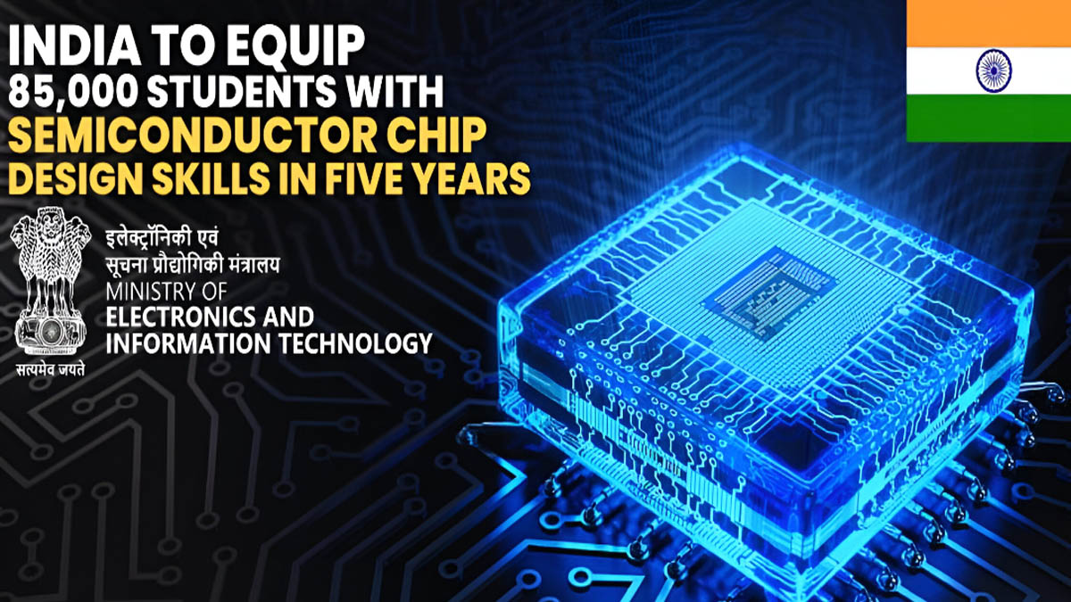
The C2S Programme, through the ChipIN Centre, aims to cultivate a highly skilled workforce, targeting 85,000 industry-ready professionals at B. Tech, M. Tech, and PhD levels specializing in semiconductor chip design. This is achieved through comprehensive training sessions, often in collaboration with leading industry partners, providing students with mentorship and unparalleled access to design, fabrication, and testing resources.
The impact extends beyond mere training hours. The ChipIN Centre facilitates real-world problem-solving, as evidenced by recent “Analog and Digital Design Hackathons.” These competitions saw students tackle complex design challenges, showcasing their innovative capabilities using the advanced EDA and cloud resources provided by the Centre. Winning teams from prestigious institutions like IIT Delhi, NIT Rourkela, IIT Guwahati, IIT Bombay, Saveetha Engineering College, and IIT (BHU Varanasi) demonstrated the high caliber of talent being nurtured.
Furthermore, the ChipIN Centre plays a crucial role in fostering indigenous chip development. Initiatives like the indigenous ‘BLDC Controller Chip’ by M/s Vervesemi Microelectronics Pvt. Ltd., developed with significant “Made in India” components, highlight the program’s contribution to self-reliance in critical technologies.
The success of the ChipIN Centre is also attributed to robust collaborations with global semiconductor industry leaders. Companies like Siemens EDA, Synopsys, Cadence Design Systems, and Keysight Technologies have extended their support by expanding access to their state-of-the-art EDA tools to a wider network of academic institutions under the C2S Programme. This collaborative approach ensures that students are trained on the same sophisticated tools used by the industry, making them highly employable.
The government’s unwavering commitment to the semiconductor mission, backed by substantial investments and strategic partnerships, is steadily transforming India into a significant player in the global semiconductor landscape. The ChipIN Centre stands as a testament to this commitment, actively empowering the next generation of engineers, researchers, and entrepreneurs to drive India’s technological advancements and cement its position as a semiconductor powerhouse.


